
Silicon Wafer Backgrinding Process manufacturer Grasping strong production capability, advanced research strength and excellent service, Shanghai Silicon Wafer Backgrinding Process supplier create the value and bring values to all of customers.
 WhatsApp)
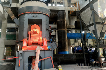
Semiconductor BackGrinding The silicon wafer on which the active elements are created is a thin circular disc, typically 150mm or 200mm in diameter. During diffusion and similar processes, the wafer may become bowed, but ...
DISCO Technical Review Feb. 2016 1 Silicon wafer thinning, the singulation process, and die strength Sales Engineering Department Abstract In recent years, the realization of the IoT (Internet of Things) society, in which anyone can ...
The TAIKO process is a wafer backgrinding method developed by DISCO. This process method leaves a ring (approximately 3 mm) on the wafer outer edge and thin grinds only the inner area of the backside wafer. By leaving this edge ...
Service Overview Wafer Preparation In electronics, a wafer is a thin slice of semiconductor material used to fabricate integrated circuits or other microdevices 1. Also called a slice or substrate, wafers must undergo a number of steps ...
2017/07/05· The optical microgauge system by means of nearinfrared spectroscopic measurements was proposed as the thickness monitoring tool in the silicon wafer thinning process. The FabryPelot interferometry and Beer''s law ...
Silicon Wafer Back Grinding Wheel Features Thoroughlymonitored manufacturing process for nearzero scratch Manufactured in clean room class: 100 ~1000 Errorproof PSD (Particle size distribution) analysis and control ...
2016/12/15· One thought on " The backend process: Step 3 – Wafer backgrinding " enrique December 15, 2016 at 7:17 pm We suggest you the UV release tape for attach wafer/glass to grind and polish. Once finish the grind and ...
Grinding Machines for Semiconductor Wafers Koyo Machine Industries developed several types of grinding machines, used in the semiconductor industry for silicon wafer manufacturing and IC production. Vertical and horizontal spindle ...
Backgrinding Backgrinding is the process of removal of silicon from the back of wafers following conventional semiconductor processing. The process is primarily utilized in thinning wafers for commercial semiconductor wafer fabs. ...
2016/03/02· めまれている· Backgrinding thin wafer debonding process, with UV dicing tape laminated.
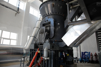
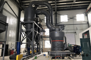
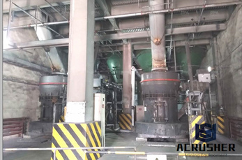
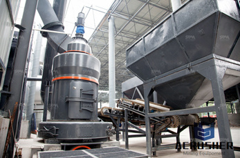
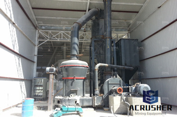
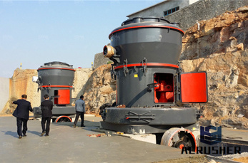
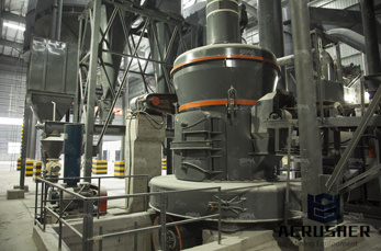
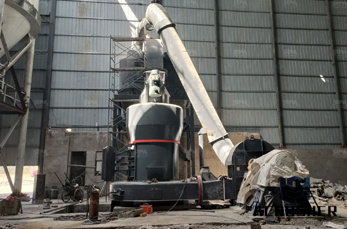
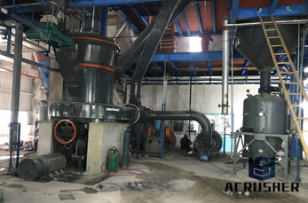
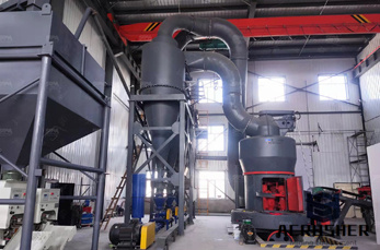
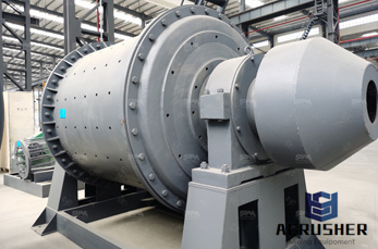
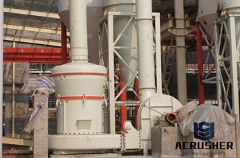
What We Do? Grinding Process Wafer offer advanced, reasonable solutions for any sizereduction requirements including quarry, aggregate, and different kinds of minerals. We can provide you the complete stone crushing and ...
ICROS TAPE is used to manufacture integrated circuits as a surface protective tape in the silicon wafer backgrinding process. ... ICROS TAPE is a surface protective tape used in silicon wafer backgrinding process for the ...
2016/02/15· null Dry etching is a new method for wafer thinning. The ADPDCE process introduced by TruSi 3 uses Ar/CF 4 plasma. The thinning rate is about 20 µm/minute and results in a uniformity 2 percent for removing 20 µm.
Back grinding is a process that removes silicon from the back surface of a wafer. AW provides grinding on our own substrates or on customer supplied wafers. We process bare and device patterned wafers with high yield and offer ...
The TAIKO process is the name of a wafer back grinding process that uses a new grinding method developed by DISCO. This method is different to conventional back grinding. When grinding the wafer, the TAIKO process leaves an ...
SiC,MEMS,Silicon carbide,GaP,GaAs,Si,Photomask,Sapphire,Synthetic quartz,Substrate,Polishing,Semiconductor,Compound,Backgrinding,Back polishing,Cleaning,Metal ... we are offering semiconductor polishing, the work of the ...
Our silicon wafer manufacturing process can be divided into two stages, namely, pulling single crystal ingots and slicing and polishing the silicon wafers. ... Pulling Single Crystal Silicon Ingots (CZ Method) In the CZ method ...
This study investigates warping of silicon wafers in ultraprecision grindingbased backthinning process. By analyzing the interactions between the wafer and the vacuum chuck, together with the machining stress distributions in ...
2014/12/02· めまれている· Polishing Processes Behind Silicon Wafer Production | Wafer World Duration: 2:30. Wafer World Inc. 2,463 views 2:30 ...
Wafer backgrinding involves thinning semiconductor wafers after IC have been fabricated onto the wafer. Semiconductor wafers go through the IC foundry processing steps on a wafer having a thickness that best supports reliable and ...
BGM300 is one of the latest WASAVI series products from Lasertec. It accurately measures silicon thickness, TSV depth and remaining silicon thickness (RST) before and after the TSV backgrinding process, a critically important ...
2014/12/02· めまれている· Wafer Back grinding coating(lamination film) Duration: 3:20. kyuseok BAE 585 views 3:20 Silicon Wafer Processing Animation ...
Wafer backgrinding is a semiconductor device fabrication step during which wafer thickness is reduced to allow stacking and highdensity packaging of integrated circuits (IC). ICs are produced on semiconductor wafers that undergo a ...
Semiconductor Material Wafer Backgrinding Double side polished wafers to TTV < 1 micron Silicon, Germanium, Gallium Arsenide, Gallium Phosphide, wafer shaping Slicing to 5" diameter Wafer edge grinding Lapping to 300 mm ...
WhatsApp)